
- AUTOCUTS
- CCD camera
- CryoMatrix® holey Grid
- Magnetic Field Cancelling System
- Vibration Isolation System
- HATA-Holder System
- PIE plasma cleaners
- Nexperion SentineL
- WET-SEM
- Temassist-Towards Automatic TEM solutions
- FEG and LaB6 filament
- Compressors
- Chiller
- Vacuum System
- High-vacuum Optical Platform for cryo-CLEM
- Quick Freeze Substitution Equipment
- Agar Auto Sputter Coater
- Coating instrument
- Cryo-FIB sample preparation
- Nanometer Pattern Generation System
Product Details
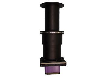
The NanoSprint15 Mk-II is AMT’s product featuring an entirely new sensor that achieves the high sensitivity required for materials and life-sciences. Its fine-pixel, low-noise CMOS sensor offers a large 15 megapixel sampling region with a high speed 32fps readout.
AMT coupled the sensor's generous field-of-view and ultra-fine sampling with AMT's high performance optics to create a system that is ideal for a wide range of applications. Users can enjoy both its excellent contrast plus the ability to zoom for
images that contain both context and detail.
Technical specifications
Sensor Size [pixels] 5056 × 2960
Phosphor Pixel Size [µm] 12.75 x 12.75
Active Pickup Region [mm] 65 x 37
Digitization 16 bit
Mounting Position On-Axis
HT Range [kV] 20–200
Optical Coupling Custom high performance lens
Lens Magnification 0.34
Lens NA image 0.32
Lens MTF at Nyquist [%] >50
Framerate for Display Image [fps] 30
Cooling 200C water
Micro Lenses Yes
Shutter Global
Exposure Time [ms] 1 - 10,000
Power 100-240VAC
Digital Interface PCIe
Vacuum Compatibility <10-7 torr
Vacuum Seals Fixed o-ring
Environment Electronics and cooling outside of vacuum
X-ray shielding limit Up to 200kV
Certifications UL, CE , RoHS
Computer OS Windows 10 Professional 64 bit
Product appearance