- AUTOCUTS
- CCD camera
- CryoMatrix® holey Grid
- Magnetic Field Cancelling System
- Vibration Isolation System
- HATA-Holder System
- PIE plasma cleaners
- Nexperion SentineL
- WET-SEM
- Temassist-Towards Automatic TEM solutions
- FEG and LaB6 filament
- Compressors
- Chiller
- Vacuum System
- High-vacuum Optical Platform for cryo-CLEM
- Quick Freeze Substitution Equipment
- Agar Auto Sputter Coater
- Coating instrument
- Cryo-FIB sample preparation
- Nanometer Pattern Generation System
Product Details
Electron diffraction offers some very attractive advantages compared to X-ray diffraction. The most important is that electrons interact much stronger with matter than X-rays do, making it possible to study extremely small crystals. This strong interaction makes multiple diffraction a serious problem, even for crystals only a few nanometres thick. Because the Ewald sphere is almost flat, many reflection sare simultaneously in diffracting conditions. This is especially true for diffraction patterns taken near zone axis directions or major diagonals. It was long thought that electron diffraction data could not be used for solving crystal structures, as is done with X-ray diffraction, because of the strong dynamical effects.
The dynamical effects could be significant reduced by rotating the electron beam around the optical axis. Dynamical effects would much less pronounced than with the conventional electron diffractions, when only a few reflections are in Bragg condition at any one moment.
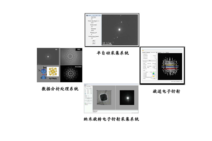
We developed a system, “Temassist”, for automatic data collections with different scientific purposes, including “Simple-EDT”, “Nano-RED”, “Digital-Precession”, “Analazer” functional modules.
Technical specifications
1. The minimum step length to reach 0.1°, increased by nearly 10 times higher than the general sample stage in accuracy.
2. Using the sample stage motion drift correction, regulate the drift error during samples rotation process, provide accuracy of diffraction values collected.
3. Using high-speed CCD camera, to minimize drift and sample irradiation time, improve the accuracy of diffraction values.
4. Accurate control the position of the electron beam, geting positioning accuracy of the electron beam within 50nm.
5. Integrated electron microscope electron beam rotation, the sample stage and CCD acquisition value, so that the integration of the system, greatly reducing the inconsistent problems between electron beam and sample position, but also to avoid errors between sample collection diffraction values and the true position.
6. This system not only can automatically collect and efficient calculate more accurate single-cell data ,but also can give users 3D diffraction dot-shape data, which would greatly satisfy the needs of analysis structural defects as a new generation of products.
Application example


